electronic Hardware
The electronic design of the Embedded Resume device is the heart of the entire project. It is the mechanism which gives the system its functionality and allows the physical world to interact with the digital.
Not only do the electronics provide practical capabilities, they also quite literally serve as a piece of my resume. It is a physical example of my work, and I couldn’t simply just cram a handful of ICs onto a PCB and be done. This was something that a hiring manager, who has very likely had hardware design experience, would scrutinize down to the last resistor, and it therefore had to be elegantly designed.
Github
The entire codebase and hardware system for this project, as well as pictures, bitmaps, and documentation can be found on my GitHub:
https://github.com/aaronv55/Embedded-Resume-Project
High-Level Requirements
Before we can even begin to start planning our system, we need a concrete set of design requirements to work from. Far too many engineering projects fail simply because goals were not well established early on, and development runs off into the weeds before a product is ever built.
In depth requirements for each module are explained in their respective sections in this article, but from a high-level perspective, I required the Embedded Resume device to include the following at the start of the project:
- Color LCD display with touch sensing
- Ability to store and read external images, sound clips etc.
- Circuitry must be physically robust and protected from hazards introduced by the user
- Compatible with both battery and USB power sources
- Means of delivering audio to the user
- External button
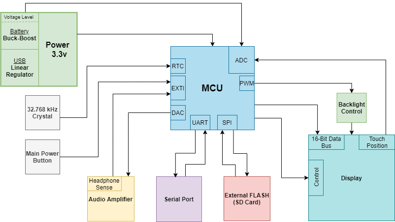
System Hardware Diagram
Schematic Capture
All of the schematic capture and layout for this project was done in KiCad 5.1.2. This is my favorite free CAD software and by far the one I have the most experience with. I played around with the idea of using Altium, since it would be more representative of the industry but ultimately decided against it. I didn’t want my student license to expire and me not to have access to any of my files at the end of the project.
Main Board
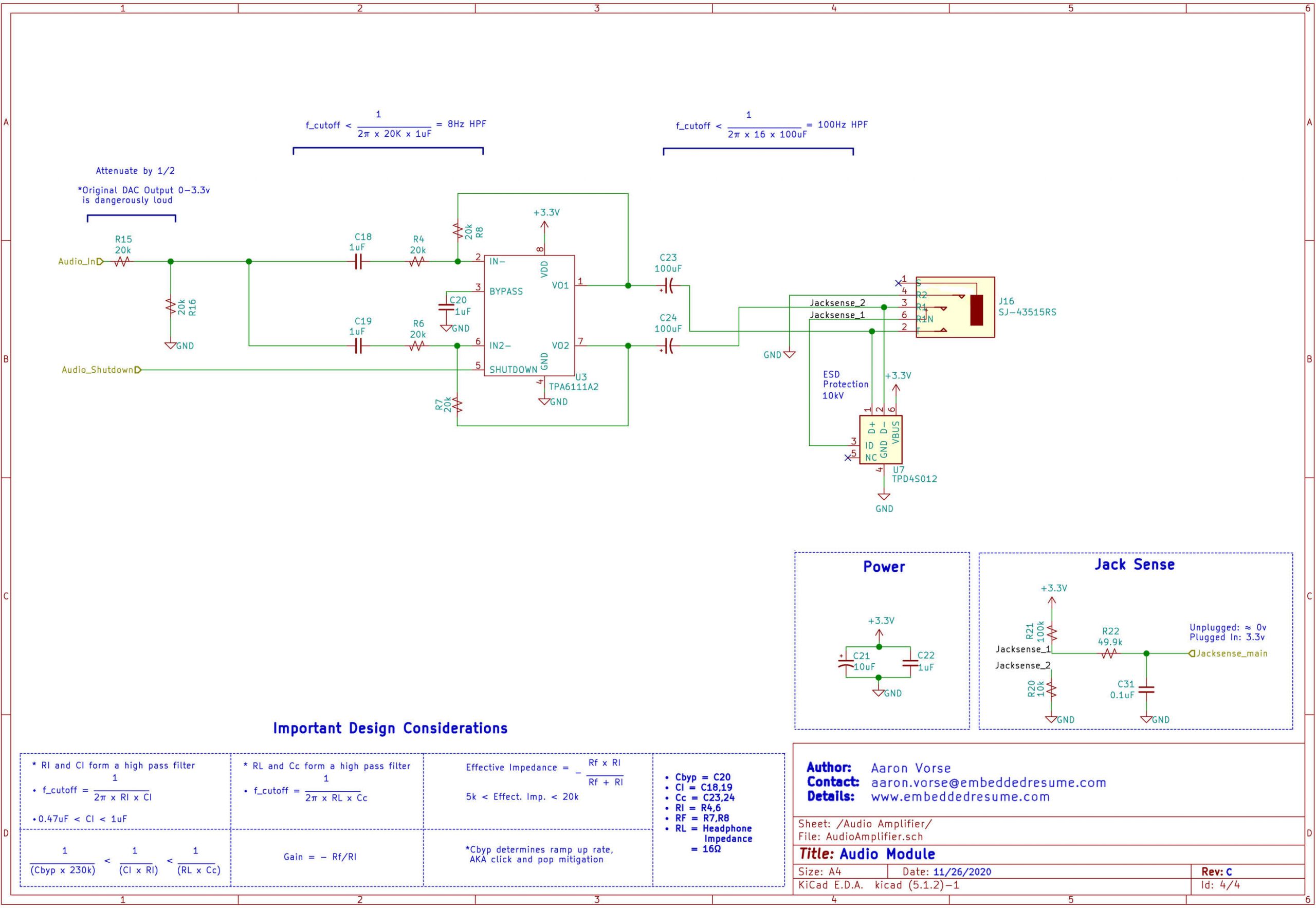
There are four sheets in the main board schematic: the main MCU and Power, USB to UART, the daughter board connector, and the audio amplifier. I like implementing these as hierarchical sheets, since it makes connections very obvious.
I often see engineers use traditional sheets and lots of global labels to connect everything together. I don’t personally like this method, since connections aren’t clear, and I usually have to waste extra time trying to hunt for global nets between sheets.
Each circuit is broken down and explained in detail in this article, but it may help your understanding to have these sheets open in a separate tab for reference.

Click on a thumbnail below to enlarge the image.
Daughter Board
The daughter board mostly serves as a means of connecting the LCD to the main board (see PCB Layout below), and its schematic therefore consists of mainly connector pinouts.
PCB Layout
Overview
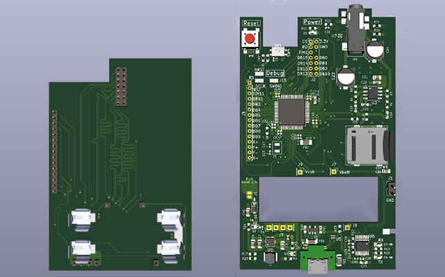
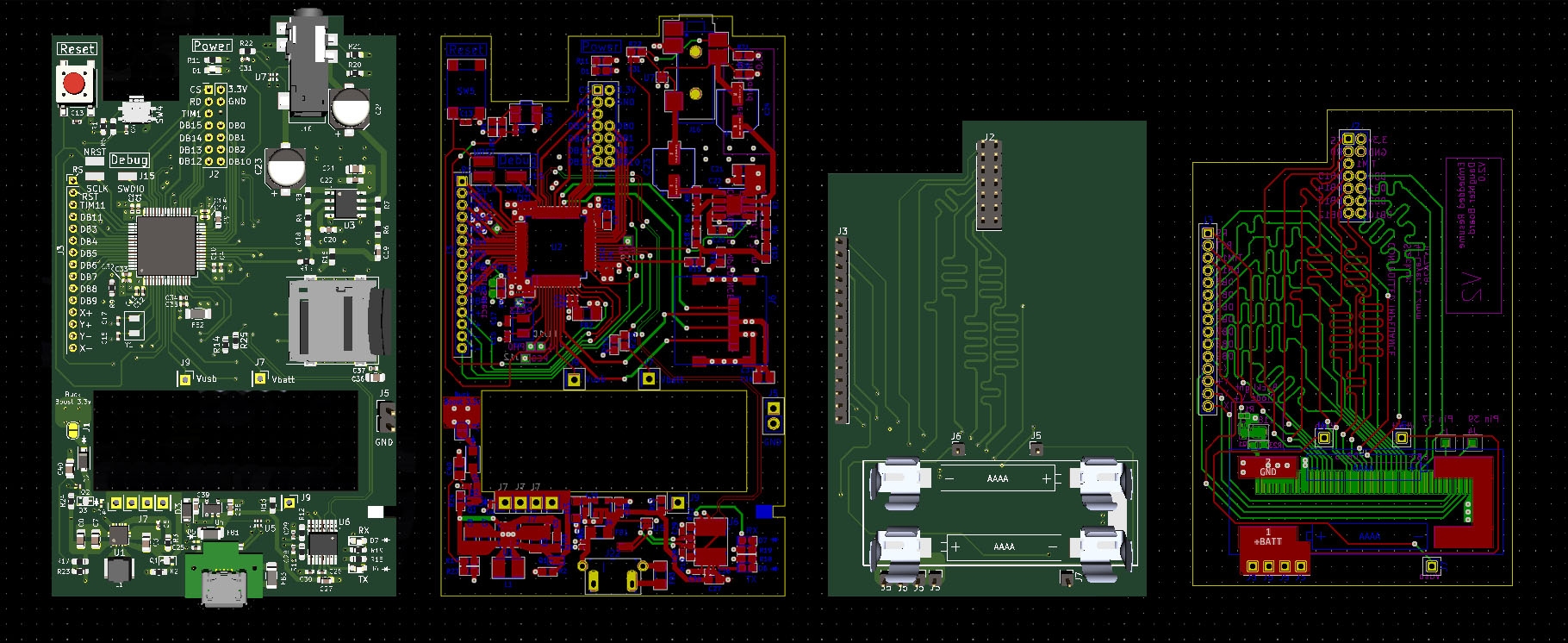
The Embedded Resume Device is made up of three PCBs which connect together to form the entire hardware system.
Board Features
- 4 Layer (signal 1, GND, power, signal 2)
- 1.2mm thickness, 1Oz copper
- RoHS-compliant, lead-free HASL surface finish
- Controlled-impedance stackup (JLC7628 from JLCPCB)
- Unless otherwise specified, all digital traces are a standard 50Ω impedance
Main System Board
This, as its name implies, is the primary PCB for the system. It contains the circuitry for the MCU, audio amplifier, power regulator, SD Card, USB-to-UART, and a handful of other sensors and inputs. This is also the board that physically slides into the rails on the device’s plastic frame (see Mechanical Design).
Daughter Board
The reasoning behind creating this separate PCB is described in much greater detail later in the article (see Display & Daughter Board). Its primary purpose is to connect the TFT display to the main board, and it also contains a bit of support hardware, such as backlight control. The board also houses the system’s AAAA battery connectors and incorporates a few traces which jump DC signals from one side of the main system board to the other.
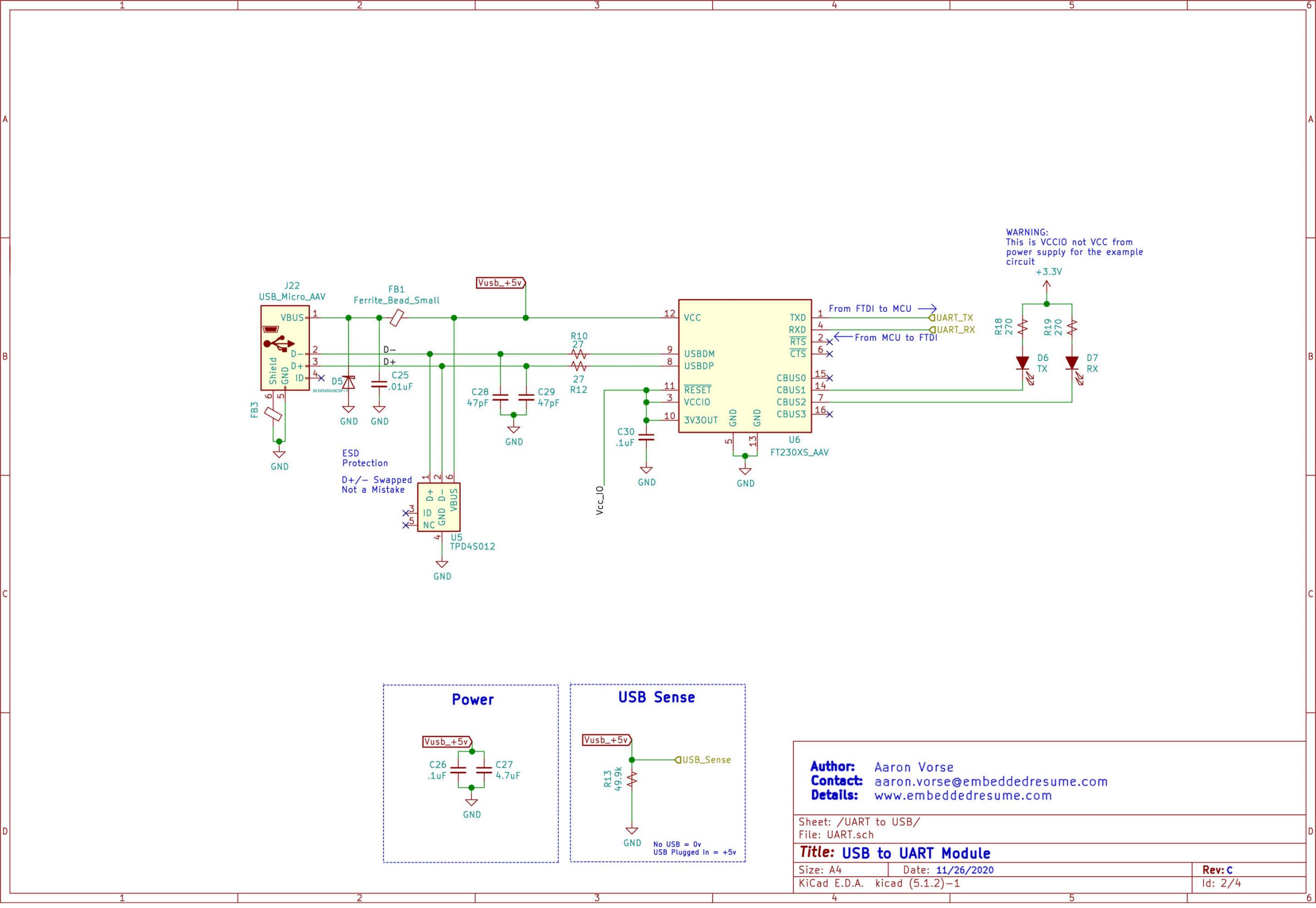
USB Chip
This tiny PCB was created more out of necessity than desire. After receiving my rev A PCBs back from the fabrication house, I realized that the USB connector was a few millimeters below its corresponding hole in the plastic frame. Since the mechanical design could not be changed, I created this tiny “chip” whose sole purpose is to physically raise the connector above the main PCB and line it up with the slot. See USB & UART for more details of my woes.
Production Goals
It’s pretty clear by looking at the main PCB that it was not designed for high-volume production. My initial thought was to lay the board out as though this were a commercial product and simulate a typical manufacturing process. I ultimately decided against the added complexity, since I knew there would only be ten total devices that would all be hand soldered and assembled.
I still wanted to show employers that I do know how to design for manufacturability (DFM), so I wrote an entire section at the end of this article detailing how I would change the design if this were going to be manufactured on a commercial scale. It includes everything from component sourcing to PCB panelization. If you’re interested in learning about my skills in a typical engineering environment, I encourage you to take a look.
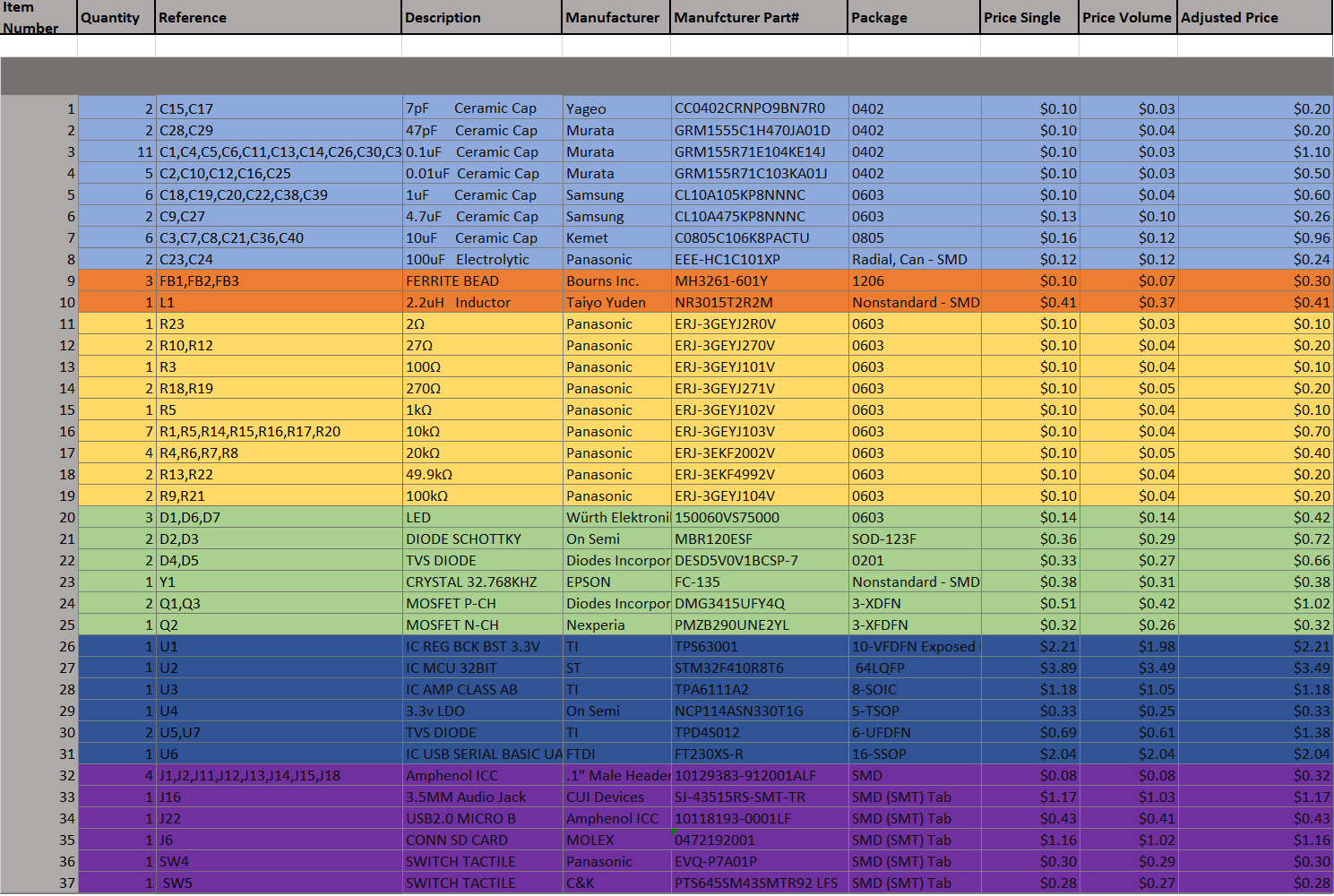
Cost & Bill of Materials
As an electrical/embedded system engineer, being able to design a board under specific cost constraints is a bit of an artform. To make a software analogy, it’s very much like selecting an optimization level for your firmware’s compiler.
If we’re making 1,000,000 units, we crank it to max and squeeze out every last cent from the bill of materials (BOM). The tradeoff here is that we vastly increase non-recurring expenses (NRE) in the form of engineering design time so that we may shave off a few million dollars of final production cost. However, if we’re only making a few one-off prototypes, this added cost and time most likely outweigh any production cost savings.
My problem with the Embedded Resume Project is that I had to do both. Some of the companies that will receive my device are large, aerospace corporations who only build very expensive one-offs and would scoff at a $50,000 FPGA. At the other end of my recipient spectrum are consumer electronics companies that would disown me for having the nerve to use 1% tolerant resistors.
I decided to split the difference and set my optimization level to medium. This meant that I would try to cut as much cost out of the design as possible, but if a $2 audio amplifier IC came along that would save me the trouble of recreating one in discrete components, I wouldn’t sweat it too much.
Soldering and Assembly
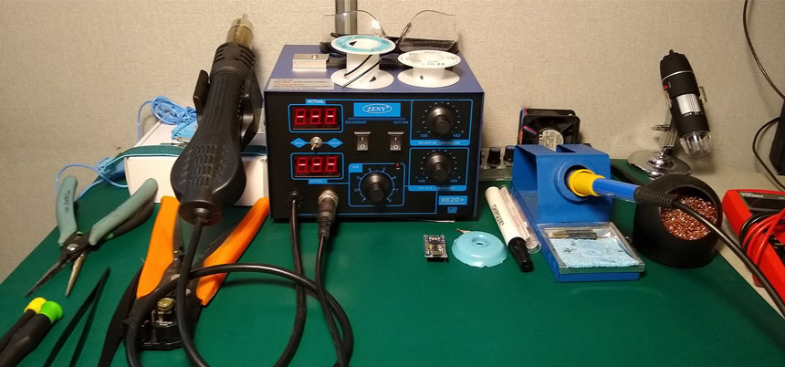
The entire soldering and assembly of each device was carried out by me personally at my home bench. At first, I entertained the idea of just having a fab house take care of assembly. After all, I currently work at a contract manufacturer and could have just run it through one of our three pick and place machines.
I ultimately decided against this, since one of the main skills listed on my resume was soldering and rework. I wanted to show employers that I was capable of modifying boards during prototyping.
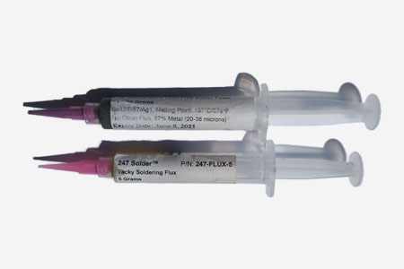
Solder and Flux
I have spent the last six years burning my hands, destroying PCBs, and learning what NOT to do when solder. Please, for your own sanity, if you are doing any kind of SMT soldering go out right now and get yourself a syringe or tub of solder paste. It makes your work much easier.
I knew that I wanted to use lead-free solder for the Embedded Resume Device to maintain RoHS compliance and, more importantly, to keep the user safe from toxic chemicals. I have grown fond of this 247-brand lead-free, low-temperature solder paste. The low-temp feature is critical, because it’s very easy to accidently roast your board and lift pads while trying to melt lead-free solder without a reflow oven.
I also chose a simple no-clean flux from the same brand. In a perfect world, I would have chosen a water-soluble type and done a full board wash. I chose to go the standard hobbyist route and just do a final cleaning with 95% IPA before the mechanical pieces went down; sue me.
Method
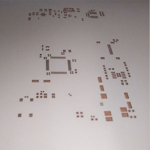
A common way of soldering SMT components quickly is to buy a stencil from your board house. This is just a sheet of stainless steel that has an exact copy of your PCB’s component footprints. At your contract manufacturer, a machine squeegees solder paste over the holes, and a perfect amount is deposited onto each pad. You can do this at home with a credit card and a bit of patience.
Although I ordered stencils with my Rev A PCBs, the pads on my board were large enough to just use the syringe for depositing solder. The majority of the board was done with this paste and my hot air rework station, and messy joints were cleaned up with flux and my iron.
The pin headers and a few other components were soldered with my iron and thin-gauge, lead-free Kester solder on the spool.
The Woes of Via-in-Pad
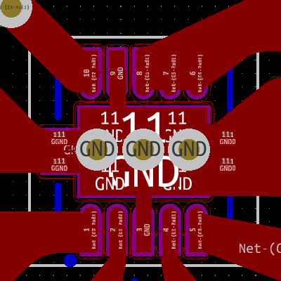
The most difficult component to hand solder was the buck-boost QFN package, simply because I used via-in-pad.
Via-in-pad is, exactly as its name entails, when you place a via inside one of a component’s pads during layout. This is generally very much frowned upon, since it introduces a whole bunch of problems during manufacturing.
The buck-boost had a large ground pad in the center of the component, and I dropped a few vias to the GND plane to dissipate heat. During soldering however, this worked too well, and I had to crank the iron’s temperature way up just to have the solder even budge. Even worse, since the pad was under the component, I could only touch my iron to the small traces on the side.
Worse still, via-in-pad is notorious for wicking away any surface solder and leaving the pad bare. If you put too much solder on however, the QFP floats a few mills above the surface, and its leads never touch their pads. This juggling act took up a large portion of the overall soldering time.
If you also find yourself in this situation, try these tips:
- Heat the entire PCB up with your hot air rework station. It doesn’t need to be hot enough to melt solder, we’re just trying to raise the entire board’s average temperature.
- Tin the pad that has vias with a small portion of solder beforehand. This should be just barely enough so that the holes of the via disappear and nothing more, or you risk making your part float.
- Use a solder tip like a knife or chisel style that makes a large amount of contact with the board. Conical or pointed tips make very bad contact and will not transfer enough heat to the pad.
- If this still fails, try doing the stencil/credit card method with your hot air gun.
Power
Defining the System Power Requirements
The first step in designing the power supply circuitry for the system was to establish an operating voltage. Since both the MCU and the LCD (two of the most important modules on the board) natively supported 3.3v, I decided that was the best option. Nowadays 5v systems are slowly starting to phase out, and boosting up from something lower, like 1.8v, would have simply increased complexity and decreased efficiency with no benefits.
I moved on to creating a rough power budget. By far, the most power-hungry portions of the system were the LCD, MCU and audio amplifier.
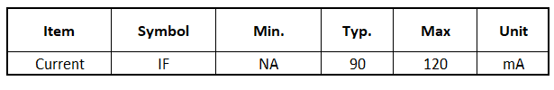
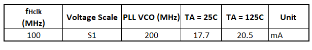
Here we can see that the LCD and MCU core will pull a maximum of roughly 120 mA and 20mA respectively during normal operation. Although the audio circuitry for this section had not been defined when I created the initial power budget, I assumed a standard 1v p-p output feeding 16 Ω headphones (roughly 60mA peak).
When budgeting for power, I always assume the worst-case scenario. This means looking at the entire system as if every part is pulling maximum current and then giving that number a bit of wiggle room to be safe. This ensures that the system will always have adequate power and that we don’t accidently brown out any IC.
We are now at around 200mA, but the real system will have pull-up resistors, LEDs, peripherals, and other ICs that will also take power. I gave plenty of room and defined my absolute worst case scenario as roughly 300mA. One last important note is that we also have to factor in the total inrush current so the board will boot up properly.
In retrospect, the final average current consumption is only around 140mA, but it is always better to overbudget than come up short months into a project.
Selecting the Battery
One of the main pain points I had early on was finding the right battery. If this were a commercial product, it would almost certainly use a simple 3.7v LiPo. Doing so would have made my life much easier and the overall mechanical design thinner and sleeker. I fought with the idea for a few days, but I ultimately decided it was too dangerous.
I did not have a team of engineers at my disposal to spend months properly testing, validating and verifying a LiPo monitoring circuit. It simply would have been negligent for me as an engineer to send off such devices. After all, I’m trying to impress potential employers not accidently set their offices on fire, right?
After going through the five stages of grief, I ultimately settled on the AAAA battery due to its small size and current capabilities. This little-known cousin of the AAA was also available in a much safer Alkaline composition.
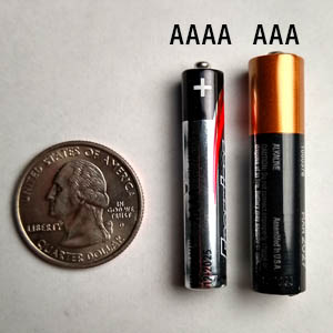
Two of these cells could just squeeze perfectly into the device’s case. In series they would get me close to 3.3v and could source a few hundred milliamps for a couple of hours; just what I needed.
Quick Review of Power Requirements
- Input of both USB (5v) and battery (2v – 3.4v)
- Output voltage = 3.3v
- Output average current > 300mA
- Output inrush current > 400mA
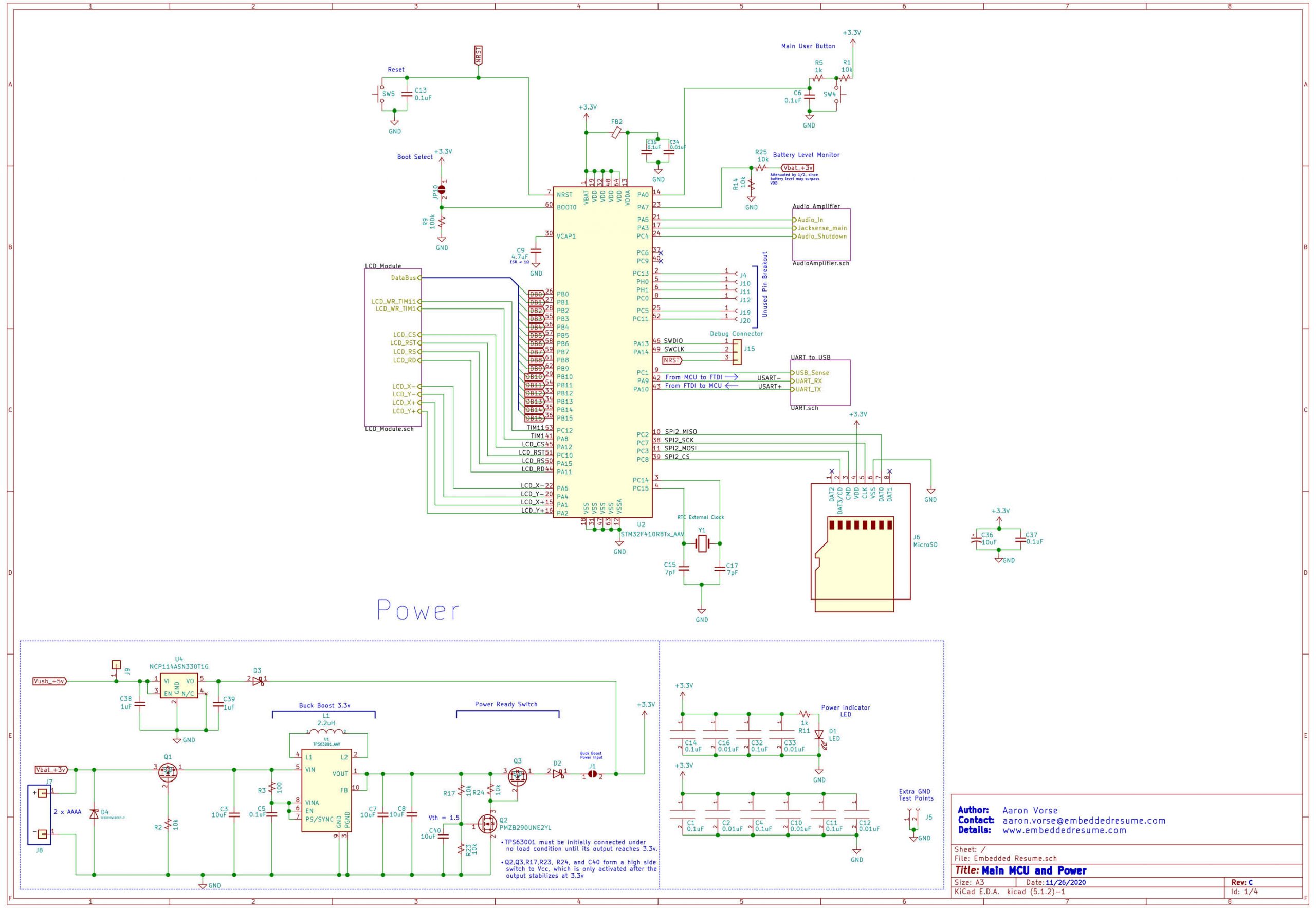
Main Power Circuit: Rev A
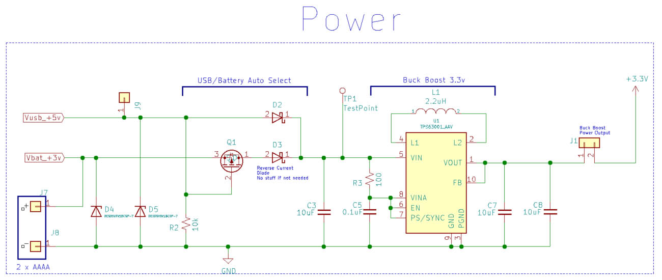
The main constraint for this section is the battery voltage. Two alkaline cells in series will generally start around 3.4v and drain to roughly 2v, meaning that we need a regulator capable of both lowering and raising voltage; we need a buck-boost. After spending a few afternoons leafing through datasheets, I settled on the TPS63001 from Texas Instruments.
It meets all our design requirements: Output current > 800mA in boost mode, input voltage range 2.4v – 5.5v, fixed 3.3v output voltage. Perhaps equally as important, there is plenty of documentation online, it comes in a compact, 3mm x 3mm QFN package, and I won’t have to sell my liver to afford it in low quantities.
Looking at the schematic above, everything to the right of C3 is nearly identical to the example circuit in the datasheet. Having dealt with grouchy buck-boost converters in the past (especially with this one operating above 1MHz), I chose to leave this as is.
The system must also be able to seamlessly switch between battery and USB power, meaning the two sources must be connected at the input to the regulator, exposing our batteries to a raw 5v. Although alkaline batteries are generally safer than LiPos, they still get grumpy if you subject them to reverse current and are prone to leak or even explode.
To avoid this, we place a p-channel MOSFET (Q1) in series with the battery input. This forms a high side switch, which automatically disconnects when the USB rail is high. I also added two schottky diodes (D2 and D3) out of an abundance of caution to further prevent reverse current in either direction.
This topology is all over the internet and electronics literature; we’re not exactly (and should not be) reinventing the wheel with our power supply.
With such a simple design, there shouldn’t be any big hiccups, right?
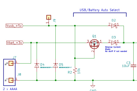
Wrong. After receiving and assembling my rev A PCBs, I connected the input power terminals to 5v and checked the output; a clean, stable 3.3v. Perfect. I shorted J1 to connect power to the main board, and…nothing. Well, not exactly nothing; I had actually fried the main processor and a handful of other IC’s.
After poking around the circuit for a few days, I found that there were two main problems which were preventing the regulator from powering up correctly:
2.
The first was the schottky diodes (D2 and D3) on the input of the TPS63001. Upon startup the chip briefly pulls a massive burst current. The diodes were essentially starving the IC before it could reach a steady 3.3v.
I modeled this circuit in LTSpice and even downloaded TI’s proprietary SPICE program, TINA-TI. Unfortunately, I could not reproduce the error in either simulation. I did however find a few forums where users claimed to have similar issues using diodes before the regulator’s input.
I confirmed this theory on both the main PCB and with a third-party TPS63001 breakout board. With an input diode, the output voltage would oscillate sporadically around 2v. When removed, the voltage would correctly stabilize.
The second was a bit trickier. The buck-boost would not power up under load. When disconnected from the system, it would correctly stabilize at 3.3v perfectly fine. Once stabilized, any load within specifications could be attached without output voltage error.
My best guess is that the system pulls too much inrush current while the regulator is still ramping up, causing it to malfunction and never reach the desired 3.3v.
Main Power Circuit: Rev B & C
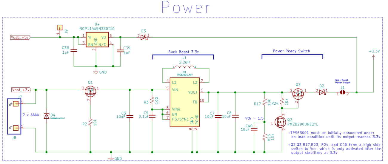
I had to completely rethink the power supply, or this device would be nothing more than an expensive paper weight. I came up with the above circuit.
I know, I know. If I had put such a design into a commercial product, I could never show my face in this town again. However, before you completely lambaste me for creating two seemingly independent power supplies for one product, let me defend myself a bit.
After discovering my two main issues, I only had a few logical options:
- Search for a brand-new buck-boost converter with similar characteristics, then waste lots of time redesigning the entire circuit and laying out a completely new power section.
- Order a multitude of different schottkey diodes, praying that one of them could provide the voltage-current tradeoff necessary to not starve the regulator. Find a way to power up under a no-load condition.
- Take out the input diodes completely and have the USB power regulated separately, then still find a way to start the buck-boost under no-load.
After careful consideration, I chose the final option. What I was really trying to avoid was finding a completely new buck-boost and wasting time redesigning the PCB. There was a good chance that it would have its own shortcomings, and I didn’t want to find myself three revisions and months into the project still battling with the power supply. I just needed something that was simple and that I knew would work.
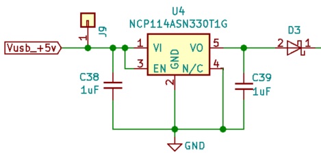
Since the USB voltage is well above 3.3v, I could simply regulate it down and connect after the buck-boost. I would still have to create a method for starting up under no-load, but half of the battle was now gone.
To lower the USB voltage from 5v to 3.3v, I chose the simplest and arguably most reliable method; a low dropout regulator (LDO). Unless Zeus himself hits it with a lightning bolt, your average LDO with correctly sized capacitors will work 99.9% of the time for a simple microcontroller circuit.
In the event that only battery power is connected, D3 prevents current from sneaking back across the LDO and creating mischief where it shouldn’t.
Now we need to take care of the second problem, making sure the buck-boost is disconnected from the system on startup. We then want some type of sensing circuit to trigger after the regulator is stable and connect power to the rest of the board.
After a bit of brainstorming, I came up with the following simple yet surprisingly effective design on my own.
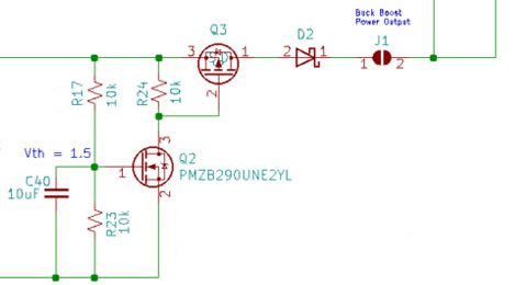
First, let’s look at Q3 and R24. Together they form a simple high side switch that is capable of either shutting off or turning on power to the entire PCB. Glossing over some complex MOSFET equations, as long as the source of Q3 (pin 3) stays less than 1v above the gate (pin 2), the transistor essentially acts as an open switch.
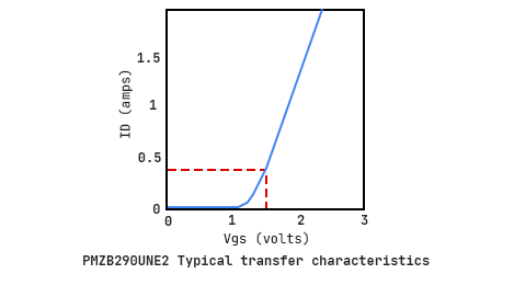
Take a look at the transfer characteristics of Q2 (an NMOS) above. It has a threshold voltage of roughly 1.5v, meaning if its gate voltage is 1.5v above its source voltage, the transistor acts as a closed switch.
Our buck boost is going to output 3.3v, and if we simply fed this into the gate of the NMOS it will trigger at 1.5v, long before the regulator voltage has stabilized. So, we use R17 and R23 to form a simple voltage divider that cuts this in half, meaning the NMOS will trigger when the buck-boost is at 3.3v, not 1.5v.
Finally, I wanted to make the design even more robust and added C40. This will form a simple RC delay and give a buffer between the time that the power stabilizes and when the NMOS triggers.
Okay, let’s see how this works in action.
- Power is applied to the buck-boost, and it begins to ramp up. Q3 is an open switch, so the main board is disconnected.
- The buck-boost voltage reaches 3.3v and stabilizes. While C40 charges, Q2 remains off.
- C40 charges to maximum voltage (3.3v/2 = 1.65v), and Q2 now turns into a closed switch. This causes the voltage at the gate of Q3 to drop to Ground.
- Since the source of Q3 is 3.3v from the regulator and its gate is now GND, the transistor turns on and connects the now-stabilized 3.3v buck-boost output to the entire system.
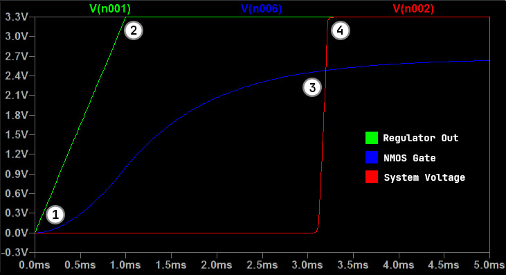
Note: I used an NMOS with a slightly higher threshold voltage (2.5v) and adjusted the resistor values for this simulation, but the idea is exactly the same for our purpose.
After simulating and verifying this design in LTSpice, I deadbugged the tiny SMT transistors and breadboarded the entire circuit.
Voila! The system would now consistently power up correctly every time. I went ahead and added the new portions of the circuit to the PCB layout for rev B and moved on.
Microcontroller Unit
Selecting the microcontroller was one of the most important decisions of the project. It was the brain behind the device and would serve, in conjunction with the firmware, to provide a rich user experience.
MCU Requirements
- Clock Frequency > 80 MHz
- 3.3v Logic to avoid level shifting
- SPI for SD card
- DAC for audio
- Multiple ADC’s for battery monitoring, touch sensing etc.
- GPIO > 32 for parallel LCD bus and general controls
- UART for debugging
- RTC
Purposely Constraining the System
The entire purpose of the project was to show potential employers that I could produce results in a typical engineering environment. I would argue that much of the field of embedded systems is simply the art of finding solutions in a resource-constrained system.
I could have simply chosen a powerful M7 core running above 400MHz with gobs of RAM, but where’s the fun in that? It’s also cheating, not representative of typical cost-constrained engineering designs, and shows hiring managers absolutely nothing about my abilities.
I decided to purposely choose an MCU that was less powerful than I normally would have selected in order to show employers that I know how to develop hardware and firmware to compensate under such conditions.
STM32F410R8T6
Before the project even began, I knew that I wanted to use an STM32. I had previous experience designing them into PCBs, they have cheap breakout boards (Nucleo boards), and documentation and examples are abundant on the internet.
After about a week of searching through nearly every cheap STM32 datasheet on Digi-Key, I chose the STM32F410R8T6. It exceeds all of our requirements:
- 100MHz clock
- UART, SPI
- Timers/PWM
- DMA
- 1.7v – 3.6v
- 64KB flash, 32KB RAM
- ADC x16, DAC x 1
- 64-LQFP
- GPIO x 50
- RTC
My main constraint here was making sure that the MCU could update the large, full-color LCD fast enough to not annoy the user. I probably could have gotten away with an M3 and some fancy DMA work, but most of them were not fast enough, and I wanted to be on the safe side.
In retrospect, I wish I would have chosen a microcontroller with enough RAM to hold at least a partial frame buffer. Also, it would have made the display a bit snappier if the MCU had a flexible memory controller (FMC) accessible from DMA.
Layout
I also purposely chose an STM32 because they’re a breeze to lay out. You can usually find them in LQFP packages which have large pin pitches and are easy to hand solder. They generally don’t need complex power rail sequencing like FPGAs and only require a few passives to boot up correctly.
Decoupling Capacitors:
– Ensure a smooth power supply and protect against brownout
– 0.01µF, 0.1µF : C1, C2, C4, C10, C14, C15, C32, C33, C34, C35
Reset Button:
– Forces a hard restart of the MCU
– SW5
Ferrite Bead:
– Helps to mitigate noise entering the analog reference pin
– FB2
SWD Header:
– Gives access to SWD interface for flashing and debugging
– J15
32.768kHzOscillator:
– Provides precise timing for the real time clock (RTC)
– Y1, C15, C17

The only thing special about this setup is that the SWD interface is accessed by three male header pins. I wanted to use the standard JTAG pinout header, but there was not enough room and adding that extra functionality would not have been worth the additional layout complexity.
Display & Daughter Board
The display for the Embedded Resume Device is the single most important hardware feature of the entire project. It gives the system its flare, allows the user to see crisp pictures of my past work, and displays fancy GUI elements for navigation.
Requirements
Defining requirements for the display was tricky because I was forced to select this component before anything else in the project had even been started. Without an LCD, I could not design the device’s case, which had to be completely finalized by March 2020 due to COVID-19 shutdowns (see Mechanical Design).
I wanted a large, color display as close to a cell phone as possible. It needed to be touch screen to give a rich user experience and eliminate the need for multiple ugly navigation buttons. The screen also had to be vertically oriented, since trying to flip a horizonal version would require the device’s case to be thick and ugly on the sides.
- At least 3.2” Diagonal Screen Size
- Dot matrix type with mid-level resolution
- Vertical Orientation
- Touchscreen capabilities
- Parallel interface for fast frame rate
- Color
Selecting the Display
The only problem with this plan is that I am not as rich as Bill Gates. Take a look at the DigiKey search results below; all of the displays that meet our criteria are in the $30 range in low quantity. Since I was making ten devices plus a few prototypes, I was not too keen on spending $360+ just for one component.
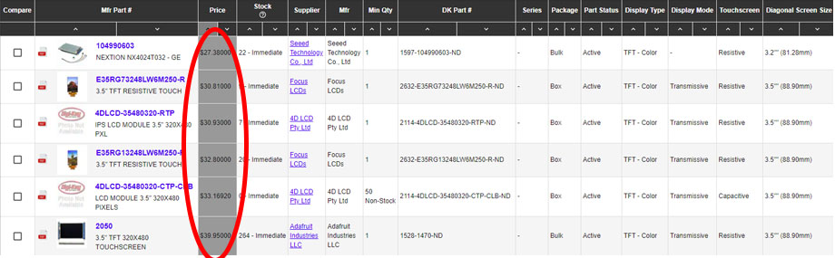
I could select a smaller, less expensive display, but that would force users to try and squint into a smartwatch-sized device. I could also probably buy something cheaper on Alibaba or Taobao, but that’s largely hit or miss and takes months to ship to the US. Since this was the heart of the project, it was the one area where I was not willing to compromise.
So, what do you do if you want a cheap, fancy display but you’re not purchasing in high volume? Well, Tom Sawyer, you get somebody else to do it for you.
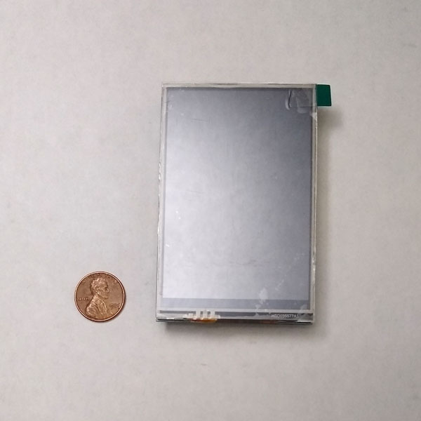
After a bit of digging, I found the TFT breakout board above which has everything I needed and more: large 3.5” screen, color, touch, 320 x 480 dot matrix, built in LCD driver, and a parallel interface. Best of all, the company has already done the hard work for us and purchased these in volume, which is why they’re able to offer them at around $18.
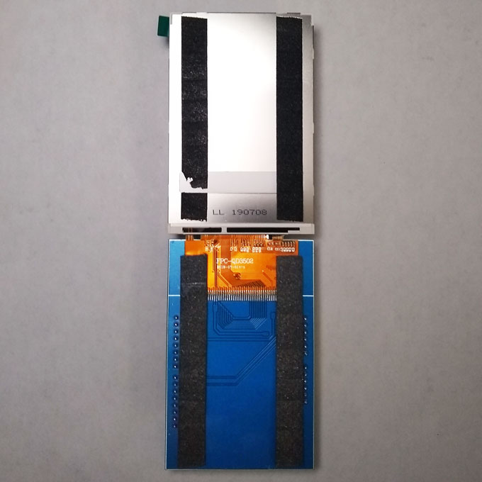
The board was originally designed for the Arduino Uno, but we only care about the display itself. I took a razor and carefully cut through the adhesive foam (upper right picture) which holds the LCD to the PCB. Now all we have to do is desolder the flex cable and viola; a $30 display for nearly half the cost.
I also kept the rest of the breakout board and used the Micro SD slot to bring up my SPI drivers before my rev A PCBs came back from the fab.
Electromechanical Woes & the Daughter Board
* It would help your understanding of this section to quickly review Mechanical Design.
At this point I had ten plastic cases already printed whose design I could not alter. I created the main PCB outline and started eyeballing potential layouts. There was just one problem; I could not find any way to incorporate the LCD.
I had designed the case so the display would be pressed in from behind and the main PCB would slide in over it. The flex cable on the LCD is only about 3cm, and there was no way (short of sawing off both rails and gluing the PCB down) it could be attached to the main board while it slid in.
I spent the better part of two weeks banging my head against the wall and googling every possible type of connector. One option was to extend the reach of the LCD by soldering on a third-party flex cable, but that would be a signal integrity nightmare. I could also run the original display cable through a hole in the center of the board to an FPC connector, but this would have nearly cut the board in half from a routing perspective.
I finally settled on a necessary solution that would not be viable for volume production. The LCD would be permanently soldered to a daughter board and both would be inserted first. The main PCB would then slide in over them and the two would be soldered together.

Schematic

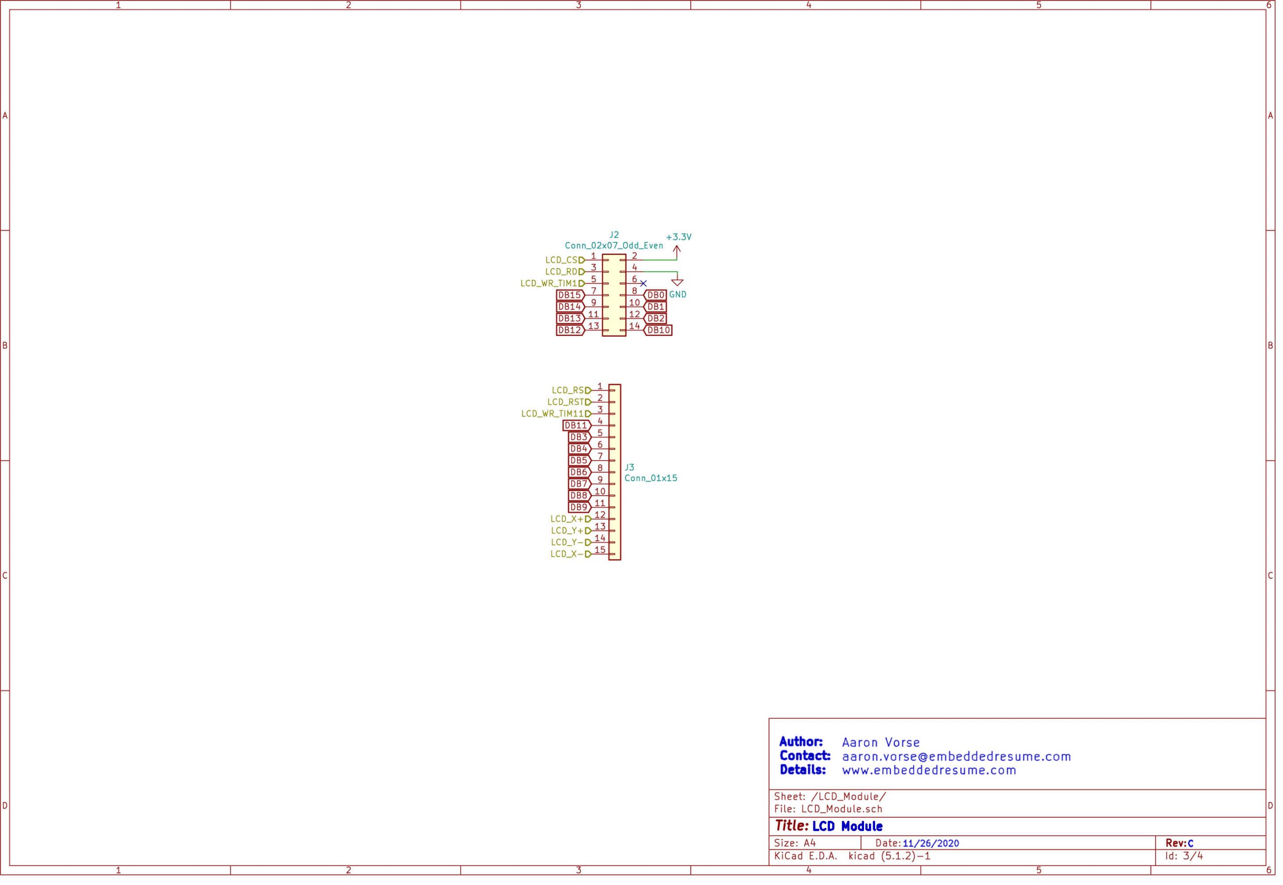
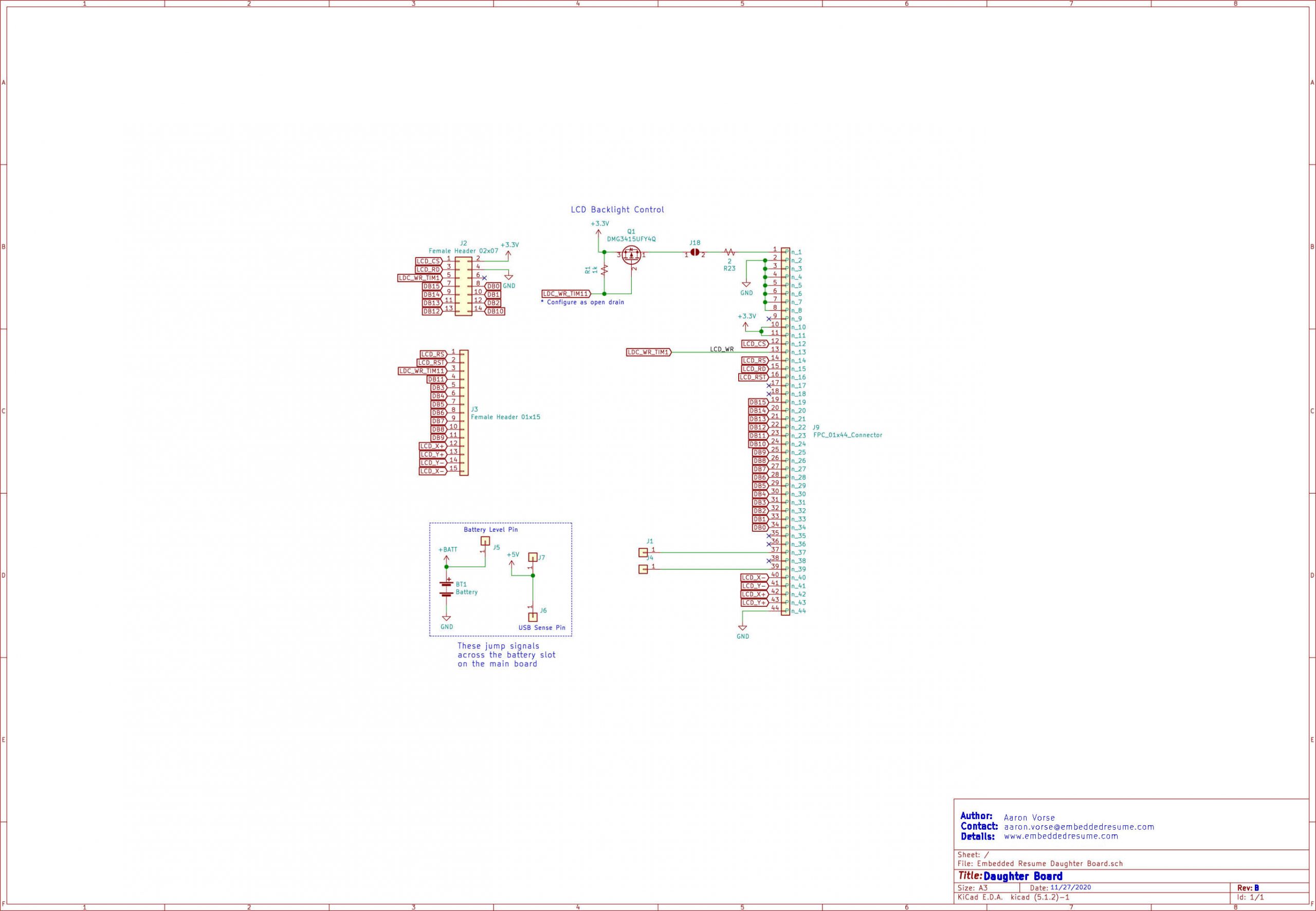
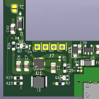
Since the daughter board is mainly just a glorified breakout board, there is not much more to the schematic than a few labeled connectors. Here we can see that all LCD control lines and the 16-bit, parallel bus are brought out to female headers. J5 and J7 are just connectors that jump the USB_sense and Battery_sense lines over the large gap in the main board.
The backlight control circuitry uses a PMOS fed by PWM from the microcontroller to dim the display. After testing the rev B PCBs however, I found that the transistor couldn’t switch the nearly 100mA load fast enough. It would do just fine at lower frequency, but that was in the audible range, and the noise was sneaking into the audio circuitry. I suppose I could have chosen a new transistor with a lower gate capacitance or simply driven the gate with an NMOS, but this was more of a wish than a necessary feature.
It’s also important to note that LCD_X -/+ and LCD_Y -/+ form a series of voltage dividers and serve as the resistive touch sensing lines for the display. Two of these are tied to normal GPIOs and the other are fed into ADC pins of the MCU.
Layout
Signal Integrity
The traces going to the LCD carry some relatively fast signals, and the board setup broke many golden rules of signal integrity. There were impedance mismatches from solder joints, and the lines had to travel between boards.
To improve signal quality, I used a controlled impedance stackup on both boards and made all digital traces a standard 50Ω. I also added footprints for termination resistors to my rev A PCBs just in case I started getting unwanted reflections. In the worst case scenario, I wouldn’t need them and could stuff them with 0Ω.
In the end, I had no signal integrity problems, and the board worked perfectly.

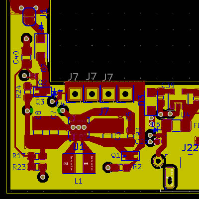
Trace Length Matching
It is common practice to ensure that all relatively fast traces going to an LCD are matched in length, with the clock pin purposely made slightly longer. This ensures that all signals arrive at the same time and settle before being clocked in.
In the absolute best-case scenario, I was hoping to get my LCD drivers running at a roughly 10 MHz clock. Anybody who has laid down DDR3 or something similar is probably laughing right now, because, in all honesty, this is so slow that trace length almost doesn’t matter. I really didn’t have to take this step, but if there’s ever a time to gild the lily, it’s when you’re building a literal electronic resume.
I used KiCad’s built in feature to match total length of each trace. I normally like to use 45° waves with 3 – 5x track width spacing because they’re easier to tune, but boy are those rounded waves aesthetically pleasing. If this were something faster, I would have probably wanted to match length for each copper layer, not just total length, but it really didn’t matter here.

Note: The layout in this picture appears to have signal traces on two copper layers directly over each other, which often leads to coupling issues. This is due to pixelization of the screenshot and is not present in the actual CAD files.