Hardware
Page 2
AUDIO
Overview
The embedded resume device was required to be able to play short audio clips to the user. I wanted them to hear me step them through pictures of my portfolio projects on the screen in my own voice. Cheap external speakers (like the ones found in children’s toys) are too power hungry for our system and often sound pretty terrible. I decided the better option would be to simply output audio through a standard headphone jack.
I wasn’t trying to win a Grammy, I just needed something simple that sounded relatively okay and got my point across. This meant that I could do away with a fancy external codec and simply feed the headphones with the MCU’s DAC.
If this were a commercial product, we would want to make the audio quality a bit better by including anti-aliasing filtering (to prevent high frequency artifacts) or at least basic low pass filters (to kill any digital noise). Once again, I kept things simple here.
By itself, the microcontroller could never power a set of standard 16Ω earbuds; we needed an amplifier. I settled on the TPA611A2 from Texas Instruments.
Gain
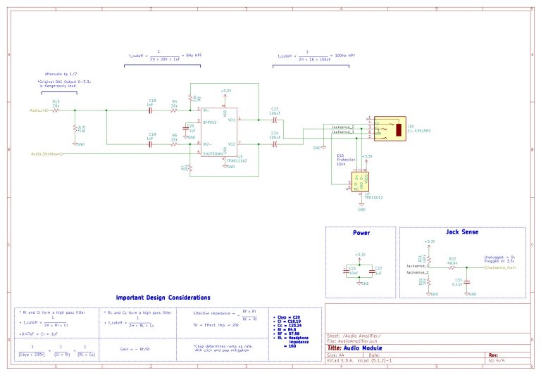
Since the MCU’s analog reference pin is tied to VCC (3.3v), the output signal coming from its DAC has the potential to swing from 0v – 3.3v. We therefore are not looking to give any voltage gain; the TPA611A2 is merely a buffer that can source the current needed to drive our headphones.
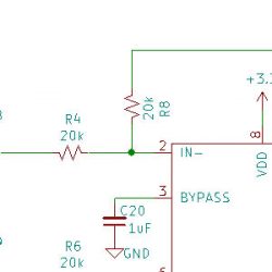
Gain is set by the ratio of R8:R4 and R7:R6. Since we don’t want any voltage gain (Av = 1), we simply make these both 20kΩ.
Important Considerations:
The datasheet highlights an important design note; the input capacitors and resistors (C18, C19, R4, R6) form a high pass filter (HPF). If we’re not careful at selecting these values, we could end up accidently cutting off lower frequencies.
Using the standard RC first order HPF equation to the right, I gave RI a value of 20kΩ and made CI 1µF. This gives us a cutoff frequency of roughly 8Hz; low enough that we don’t have to worry.
The HPF formed at the output is a little trickier simply because RL (our 16 Ω headphones) is many orders of magnitude smaller than our input resistor. This means that we must compensate and make CL very large, 100uF in our case.
I would have liked to make this even bigger, since its resulting cutoff frequency of 100Hz is a bit high, however doing so would have required physically large capacitors.
Safety Concerns:
Originally, rev A was feeding the amplifier directly from the DAC (0 – 3.3v). After flashing the MCU with my DAC driver, I uploaded an example audio, put the headphones in my ears and plugged them into the PCB.
Let me tell you; nothing quite makes you rethink safety like the audio of an opera singer piped directly into your skull at 3.3v, line-level voltage. I couldn’t hear much of anything for the rest of the evening.
With my ears still ringing, I pulled up the schematic and added R15 and R16. These form a simple voltage divider which attenuates the original audio signal. This ensures that the audio will not leave the MCU at a dangerous level, even if the firmware glitches and the DAC hits its upper voltage rail.
If I’m being honest, this is only about a C- safety rating since the amplifier itself still has the potential to output 3.3v if it fails. If this were going into a commercial-volume product where Monte Carlo starts to matter, we would certainly want to put at least a zener diode on the output to prevent overvoltage.
Jack Plug Sense:
The final portion of the audio module actually has nothing to do with the signal itself. When a user plugs in a pair of headphones, we want it to register on our device and display a fancy GUI symbol. This circuit is strictly used to detect when something is plugged into or removed from the headphone jack.
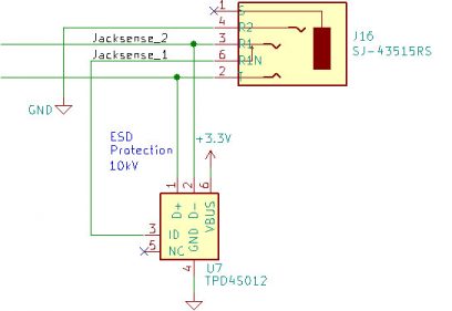
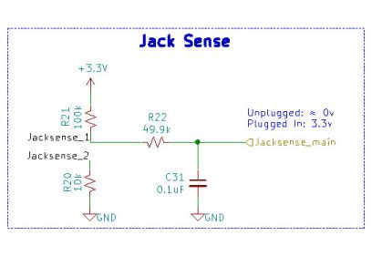
In the schematic above, pins Jacksense_1 and Jacksense_2 are shorted together when nothing is inserted into the connector. This means that resistors R20 and R21 form a voltage divider from VCC to GND, with their center node sitting at roughly 0.3v (logic zero).
When headphones are inserted, the connection between Jacksense_1 and Jacksense_2 is broken and there is no path to GND. R21 becomes a pull-up resistor and the Jacksense_main pin goes high (logic one). By feeding an external interrupt pin on the MCU, the system can keep track of whether or not headphones are plugged into the device at all times.
R22 and C31 form a simple low pass filter (LPF), which debounces the input in order to avoid causing the MCU to rapidly trigger interrupts.
Layout
Noise Reduction:
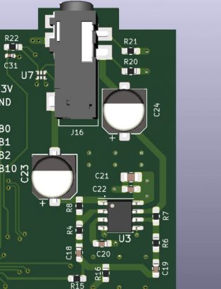
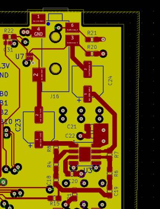
Since the audio circuit is by nature analog, I kept it in its own section of the PCB separate from the digital portions and as far away from the switching power supply as possible. This helps prevent noise from the digital circuitry from sneaking into the amplifier and causing audible distortion.
For the same reason, I also made all traces as short as possible and threw in a few extra vias to GND around sensitive lines to try and further illuminate noise entering the audio signal. Other than that, I mostly followed the suggested layout from the datasheet. Since audio is low frequency (generally sub 30kHz), signal integrity was not much of an issue here.
The final result was a nice, clean audio portion that produces virtually no audible noise.
Separate Ground Planes :
(We’re all friends here)
Alright, I don’t want to start any fights, but we should really talk about ground planes. Since the Roman times graybeards have been clashing, fiercely so, about whether to separate digital and analog grounds on a PCB. One of the main arguments is that only connecting them at a single point prevents noise from crossing over to either section.
After reading page after page of bloody forum disputes, I decided that since my board was fairly basic (no RF etc.), I would simply keep a solid ground plane for both analog and digital sections.
USB & UART
An important tool in any embedded system engineer’s toolbox is the ability to peer into the processor. Being able to see what the system is doing in real time and receive feedback vastly speeds up development time.
We want the ability to send and receive data between our workstation (laptop, desktop etc.) and our system (processor on the PCB); we need to implement USB. Our firmware was already being developed with the ST-Link debugger/programmer, which gives us this capability and much more. Why bother using something else?
- 1. The ability to debug the system when it is not attached to the debugger, as it would appear in the wild, is an extremely powerful tool.
- 2. At this point, I was still unsure whether I wanted to implement a bootloader. I would prefer to just include the hardware to facilitate one from the start, rather than need something further down the road and not have it.
- 3. There was already a micro-USB connector on the board to serve as a power source.
- 4. Adding an external serial port to a PCB nowadays is so simple, it’s almost criminal not to have one.
There’s absolutely no way our tiny microcontroller could handle an RTOS and full USB stack, so we’re going to cheat a little. FTDI is famous for its family of converter ICs that take USB in on one end and translate it to your favorite protocol on the other. We’re using the FT230XS-R, the 3.3v logic-level flavor of their USB to UART converter.
I’ve used these in the past, and I specifically chose one here because they just simply work. There’s little more to getting a virtual COM port on your PC than whacking a chip down and tying it to a spare UART. They also have royalty free PC drivers that are easy to install and make setup simple.
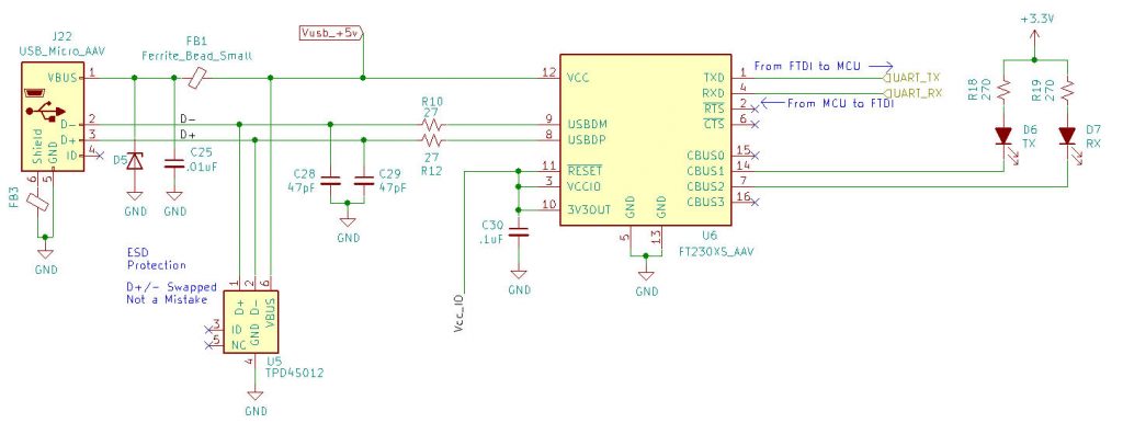
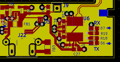
For the most part, the schematic above is identical to the datasheet. The important parts here are the capacitors (C28, C29) and termination resistors (R10, R12) on the D-/+ lines. I will explain this in detail later (see layout below), but the SparkNotes version is that these components ensure that the chip and PC are sending nice, clean signals to each other.
The ferrite bead (FB1) is used to stop as much high-fequency noise as possible from entering the power supply. TX and RX are the serial data lines and are tied to a UART on the STM32. D6 and D7 are merely LEDs that indicate the level of TX and RX at any point.
We also want the system to know when it is connected to USB, so the simple pull-down resistor circuit (right) is included. The USB_Sense line feeds a 5v-tolerant GPIO on the MCU, telling it if USB is present.
Layout
The only real thing to watch out for with the USB module is the board layout. The FT230X supports USB2.0, which can potentially exceed speeds of 400MB/s. This is fast enough that if we’re not careful, we could render our signals useless.
A Crash Course in Transmission Line Theory:
If we just threw our FT230X chip on the PCB and connected it any which way, our USB communication most likely wouldn’t work. When signals on a PCB start to get into the tens or hundreds of megahertz, care should be taken to ensure signal integrity.
Although this is an entire field one could dedicate a lifetime to, for our case we are mostly concerned with three topics: impedance, ground planes, and trace length.
Impedance – We like to think of wires and PCB traces as perfect conductors with no resistance, but this is not the case in the real world. At high frequencies, traces act like transmission lines and have impedance.
To make a very long story short, in most cases you want the output impedance of your source (our PC in this example) to be exactly the same as your load (the FT230X’s D+/- pins). If the two are mismatched, reflections can occur, turning our nice, clean signals into garbage. This is the reason for the termination resistors mentioned above.
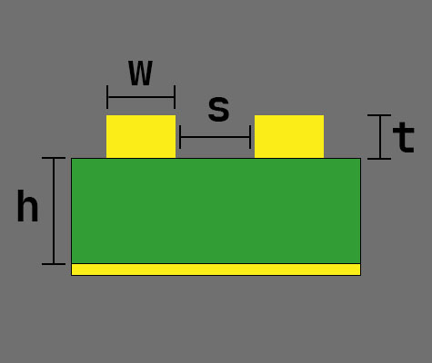
That’s not the end of the story; we also have to worry about single-ended and differential impedance. Single-ended impedance is affected by the relationship between a PCB trace’s thickness (t in the diagram to the right), width (w) and distance from the ground plane below it (h). Differential impedance involves the same factors but also includes the distance between two parallel traces (s).
Okay, so what does this all mean? The USB2.0 specs require standard 45Ω and 90Ω single-ended and differential impedances respectively. I’m glossing over a lot of important details here that you can (and should) go learn about, but the takeaway is this; if we want our chip to work correctly, our traces had better conform to these USB impedance standards. I cheated and used my board house’s calculator in conjunction with one of their impedance-controlled stackups.
My USB Trace Dimensions:
h = 0.2mm, w = 0.413mm, t = 0.035mm, s = 0.25mm
Ground Planes – We also have to pay close attention to our ground planes. Our transmission lines should have a solid, unbroken ground under their entire lengths. If not, their impedance will not be uniform, and we will get reflections. Since we’re using a 4-layer board this is not a problem, as the entire layer below the top signal layer is dedicated to GND.
Trace Length – A final concern is the actual length of the transmission lines. Although we like to think of digital signals as instantaneous, this is not the case at high frequencies. If we have the exact same high-speed, digital signal on trace A as trace B, but trace B is 100m longer, the signals will arrive at their endpoints at different times.
To avoid this, we must make sure that both trace lengths remain the same. Luckily, KiCad and most modern CAD tools have built in software to make this easy.
USB Chip:
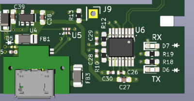
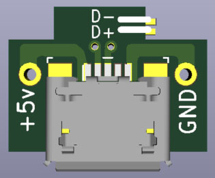
After getting my rev A PCB’s back I realized my micro-USB connector was sitting about 2mm below the cutout in the device’s case. Since I couldn’t change the mechanical design, I had to improvise and create a tiny daughter board that would lift the connector above the main PCB.
Although this breaks all the rules I just went over (impedance mismatches from solder joints, board-board high speed signaling etc.), the final design works perfectly.
A Quick Final Note:
If you look at the layout, you will notice that the UART side of the FT230X is also routed as a differential pair. If you’re an electrical engineer reading this, you’re probably shaking your head right now. This is not, and should not be routed as a differential pair, but sticking these two traces together made layout a bit easier through the congested parts of the board. I was using very low baud rates and never sending and receiving data at the same time anyways.
SD CArd
One of the main features of this device is its ability to display real, full-color pictures showcasing my previous projects. The only problem is that our system’s microcontroller has 64KB of onboard FLASH. To put this into perspective, if there was absolutely no firmware and all this memory was used for 24-bit pictures, we could only store about 1/10th of a single image.
In order to pull this off, we’re going to store our large images and sound clips on external FLASH and import them when needed. One of the industry-standard methods is to use an external FLASH IC. This plays out much like Laura Numeroff’s book IF YOU GIVE A MOUSE A COOKIE:
- If you give an engineer an external FLASH IC, she’s going to ask for an in-circuit programmer
- When you give her the programmer, she’ll probably ask you for a separate toolchain
- When she’s finished setting up her toolchain, she’ll want a special file formatter
…you can see where I’m going with this.
The added non-recurring expense (NRE) incurred by this complexity makes sense if we were making 1,000,000 of these and trying to shave every penny off the board cost. Since we’re only building a few of these, we can make our lives vastly easier by just splurging a bit on an SD Card.
We don’t have to worry about setting up a toolchain nor figuring out a physical means of uploading files. SD Cards also natively use the FAT file system and their API is extremely simple and well documented. This means we won’t have to waste time in the weeds developing file system drivers.
Layout
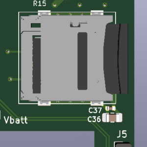
I chose a MicroSD Card holder that would allow me to drop one in from the top, since sliding it in was not an option in the tight space. The only other components in this section are a few decoupling capacitors.
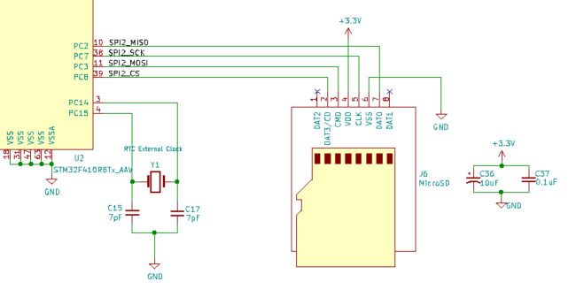
Since our MCU doesn’t have a native SD peripheral (although they are common nowadays, shop around if you prefer one), we are going to use SPI. Layout is as easy as throwing the connector down and tying our SPI2 peripheral to it. I also made all traces going to the card a standard 50Ω controlled impedance to avoid signal integrity problems. (see A Crash Course in Transmission Line Theory above)
ESD PROTECTION & REVERSE POLARITY
You pesky users you; always trying to destroy my embedded systems.
All jokes aside, protecting circuitry from hazards in the environment is something every engineer should be thinking about. From potential security risks to lightning strikes, threats should always be in the back of our minds when designing robust systems. This also works in reverse; dangers that our system could present to users (see Selecting the Battery) are equally important.
Electrostatic Discharge
When I was little, I used to run all over the house in my socks then shock my brother. Although I didn’t know it at the time, this is called electrostatic discharge (ESD), and it is dangerous to our hardware systems. There are all sorts of standards, ratings, and varieties of ESD, but at its core it is the rapid discharge of static electricity from one surface to another.
When an IC is struck by ESD, the shortest path to ground is often through its microscopic transistors, causing severe damage. This is why I am required to wear an ESD protection strap at all times during work. To avoid this hazard, we incorporate special circuitry into our PCBs specifically designed to protect against such threats.
The first step to protecting the Embedded Resume Device was to identify its weak points. These are areas where the user will come into close or direct contact with the PCB. If we’re not careful, they could unknowingly send a shock through one of these points and destroy the hardware, à la Luke Skywalker and the Death Star.
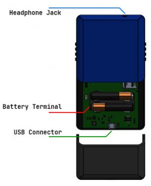
Looking at the diagram on the right, there are three main areas of concern: the headphone jack, the battery terminal, and the USB connector. These are especially dangerous because the user, who could be charged with static electricity, will be plugging in a foreign object (headphones, batteries, USB cable) and either their body or these items could discharge.
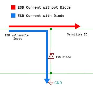
Luckily for us, the solution is very simple. Looking at the diagram to the lower right, we can see that to mitigate ESD, a transient voltage suppression (TVS) diode must be placed between any vulnerable inputs and GND. Although not completely accurate, it helps to think of this as a Zener diode which can handle large voltage spikes.
Its breakdown voltage should be just slightly higher than whatever voltage you expect your system to put on the line (5v for USB power for example). When an ESD event occurs, the line can experience thousands of volts, causing the diode to breakdown and essentially create a short to GND. The dangerous current is shunted away from the sensitive ICs on our PCB and damage is avoided.
I used regular TVS diodes for the device’s battery inputs and special USB diode array ICs (a fancy way of saying multiple diodes in one package) for the USB and headphone inputs.
Reverse Polarity
The second thing we have to protect against is reverse polarity caused by the user’s own actions. Think for a moment what would happen if they accidently inserted the AAAA batteries backwards. Our system GND would now become 3.4v and our VCC would be 0v.
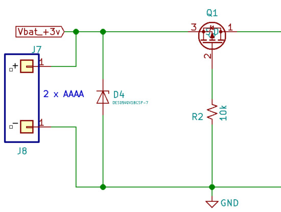
This could have undesirable or even dangerous consequences, such as the buck-boost getting hot, electrolytic capacitors popping, or at the very least destroying many of the chips on the PCB. To avoid this I placed Q1, the same type of PMOS used for our main power switch, across the battery input terminals.
If we remember our MOSFET equations, so long as the source pin stays no greater than Vth (threshold voltage) above its gate, it will remain an open switch. If we accidently plug in the batteries backwards like the example above, the gate voltage will actually be greater than the source voltage. Current will be cut off from flowing into the PCB, and the system will be saved.
TESTING JIG
During assembly, the Embedded Resume Device’s two circuit boards are soldered together in such a manner that (short of sawing them both in half with a Dremel) they cannot be removed. Now image the nightmare scenario that would unfold if we discovered a hardware bug AFTER permanently fusing them together.
To avoid this, we’re going to form a set of test procedures to validate that every unit is functioning properly. As a hardware engineer, it is standard operating procedure to send these to your contract manufacturer (where I work currently), so they can ensure everything is working correctly before assembling your final units.
If I’m being honest, this section is really just me showing potential employers that I know how to design for manufacturability/testability and carry a product through volume production. There is also a section on the Software page explaining how each submodule is tested.
Battery Emulator
One of the key hardware modules on our board is the buck-boost IC and battery voltage monitor on the STM32. To verify that these systems are working properly, we’re going to trick the hardware into thinking it is running off a real battery.
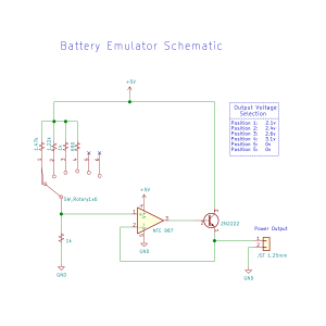
This means that we need a repeatable, constant voltage source which can provide the 100 – 200mA our system draws. There are a million ways to do this, and I designed the circuit above from junk in my spare parts drawer in a well-thought-out manner.
To summarize, a simple voltage divider (with selectable resistor values) is fed into an op amp, which acts as a buffer. It can only source a few 10s of milliamps by itself, so I added a BJT to the output in a voltage follower configuration to give it some muscle. The result is a power supply with selectable voltages capable of sourcing a few hundred milliamps.
Just a warning for anyone planning to use this circuit, it is far from the best constant voltage source. There are a lot of factors that could cause the BJT to fall out of its operating region and start acting weird, but for our simple test jig it works.
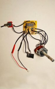
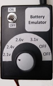
I soldered everything up on some perf board and stuck it in a fancy case for the test jig.
Main Test Jig
Along with your tests procedures, you’re typically going to send your contract manufacturer (CM) a piece of hardware known as a test jig. This is a custom set of mechanical and electrical apparatuses that plug into your PCB and position it perfectly for undergoing testing.
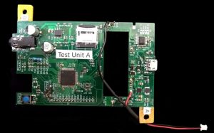
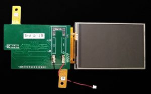
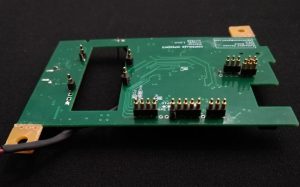
Since we have to verify two boards (the main board and the LCD daughter board), I simply made one of each a PCB test unit. For example, this means that all production main boards will be tested with the LCD daughter board test unit and visa versa. Note that the picture of test unit B was taken before its pogo pin header was soldered on.
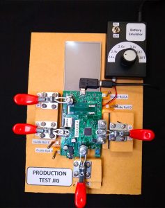
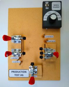
The test jig itself consists of a ¼” sheet of wood and four toggle clamps with soft rubber heads. There are also a series of guide rails which perfectly mate to the guides on the PCB test units. During production testing, the board under test is placed directly over its corresponding PCB test unit and the clamps force it onto the pogo pins below, ensuring a good electrical connection. Let’s see how this is used with an example.
If we were testing main boards for production, we would first slide the PCB test unit B (the daughter board test unit) onto its corresponding guide rails. We would then position our production board directly on top of this, aligning the pogo pins of the test unit with the header footprint of the production board. Finally, we would lock the clamps down, and the board would be ready to undergo testing.
Volume Production
As mentioned above, it’s pretty clear that the Embedded Resume Device was not designed for high volume manufacturing. I thought it would be a good exercise to outline a few steps I would take if I were making, say, 10,000 of these. This section is admittedly less of a how-to and more me showing potential employers that I know how to design for manufacturability.
Component Selection
Individual Cost: "You bought what?!"
Since I was only making a few total units, I was able to greatly speed up development time (NRE) by designing in a few fancy chips. If we were making 10,000, we’d probably find ourselves in front of an angry project manager asking why we needed a $2 buck-boost.
Simply put, if we’re building something we know will be produced in volume, we design our system in such a way as to squeeze every last penny out of the BOM. Sure, we’ll incur the added upfront cost of engineering time, but the savings in materials far outweighs this. This means that we build some of our fancy ICs with discrete components, look for other implementations, and cut out features from the final product (sorry marketing team).
BOM Consolidation
It’s also critical to make sure that we’re using as few unique parts as possible, which helps us throughout the manufacturing process. This means that while designing our boards (and ideally not in retrospect) we try to reuse components as much as possible. For example, let’s say we have two completely separate subcircuits that both use pull-up resistors. Sure, we could make one a 10kΩ and the other a 5kΩ, but it would be much better to set them both to 10kΩ.
Upfront, it saves us money on the raw materials. When purchasing from a vendor (like Digikey, Mouser, etc.) or directly from a supplier, you will almost always get a discount when buying larger volumes. That’s why, you can often get 10 components cheaper than you can get only 8.
Another less obvious benefit is during assembly. When your boards are being populated at your contract manufacturer, they get put through a pick-and-place machine, which is responsible for taking every component on your device from a reel and placing it onto the PCB. These only have a limited number of “feeders”, meaning that they can only hold so many unique parts at one time. If you exceed this number, the boards will have to get run through the machine for a second pass. Your CM can do this, but they will send you a nice, upgraded bill to go along with it.
Size
A quick note about component sizes; although you can design whatever crazy new package and size into your board that you like, you probably shouldn’t. This is due to the fact that it can make manufacturing costs increase.
For example, I put a few 0201 parts on the Embedded Resume Device as a shameless way to demonstrate my hand-soldering abilities. Although it’s getting more and more common nowadays, not all CMs (especially cheaper ones and those offshore) have machines that can handle such small parts. If I were making this device for production, all 0201s would get changed to 0402s or 0603s.
Panelization & PCBs
As mentioned above, your final production boards will go through various machines and processes before they are finished. If we had each of our 10,000 boards individually cut out and just chucked them into the pick-and-place, we would be very displeased with the cost and results. To have things go smoothly, we’re going to create PCB panels, which simply means that we’re going to take our single board and repeat it multiple times over a larger sheet (panel).
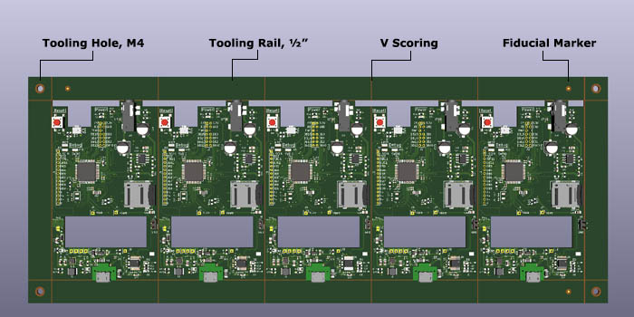
I made a mockup in KiCad of the main board for the Embedded Resume Device above, which consists of five individual PCBs. A panel must have a few features to ensure it can actually be assembled.
Spacing
Although I didn’t do this for the mockup, there should be at least 3mm from the edge of the board to any component.
Tool Rails and Holes
We need to design something called a rail, which is effectively just a blank piece of material at the edge of the board. Your CM will tell you how they like this, but it is usually at least ½” and is used by various machines to manipulate the board during assembly. The tooling holes are also sometimes used to hold the PCB down.
Fiducials
Physically, this is just a dot of copper surrounded by a circular solder mask keep-out zone. It serves as a target for the pick and place machine to lock onto in order to perform zeroing and calibration. Ideally you should have three fiducials (1mm copper, 3mm solder mask pulled back) spaced in three of the four corners of the board as far apart as possible.
Some boards which require greater accuracy also include fiducials on each individual board itself, and for boards where extreme precision is needed (300+ ball BGAs, fine-pin-pitch parts), fiducials can be placed on diagonal corners of the part itself.
Removal Method
So now that our finished panels have popped out of the reflow oven, we need some way of separating individual boards. The two most common are mouse bites and V scoring (googling these would help wonders here). These methods are carried out at the board fabrication house while the PCBs are being made and not at your CM. I try to avoid mouse bites in my designs because they leave a nasty edge on the boards and can lead to support problems during manufacturing.
Since our boards are nearly perfectly square, I used v scoring for the majority of the mockup. For this method, your board house uses a special machine to make a v cut along the top surface of the panel from one side to the other. This gives us a nice score line that we can use to physically break each PCB away from each other. This method is also good for high volume manufacturing because we don’t have to waste any space (material = money) in between boards.
Surface Level
One last quick point is how level your boards remain during assembly. There are two main problems here, rigidity and heat resistance. If we put 30 small PCBs in one panel and only connected them with two mouse bites each, the entire board would not have enough structural support and would become flimsy. When it went in the pick and place, it would bow causing all sorts of terrors, mainly misplaced parts.
Although not very apparent, the surface finish of your board can greatly affect how it will react while going through heated processes. HASL finish is cheap but can sometimes lead to less-than-ideal level surfaces. When your board goes through the reflow oven, this uneven surface can cause parts (like BGAs) to make poor contact or float on top of their pads.
Furthermore, uneven copper can have the same result. If you’ve ever seen PCBs with large, unrouted sections that still have copper pours or dithering, it is most likely for this reason. If a PCB has a very large section of copper, let’s say a power plane, on one half and absolutely nothing on the other, the uneven heating will cause the board to bow and give us problems.
Testing
If you take a look at the testing procedures for the device, you notice that there are far too many steps involving the operator. If we were making 10,000 of these, that means some poor soul(s) will have to sit down and run through our checklist to make sure each one is working properly. Here’s the thing; human beings are terrible. Sorry, let me rephrase that; human beings are terribly inaccurate.
It’s very possible that 7 hours into a shift the operator’s eyes glaze over, and your oh-so-broken unit accidently gets passed. Furthermore, people cost money, lots of money, and having somebody sit down and test every product will make your overhead soar.
If I were building the test jig and procedures for our hypothetical 10,000 units, they would ideally involve the operator pressing a button once, waiting for automated testing (Raspberry pi, etc.) to finish, then receiving a giant pass or fail sign.
